Information about our terrestrial design progress vs our flight design progress, and why we will have a new development board in Remote Labs West.
Haifuraiya is our microwave-band amateur radio satellite and terrestrial transponder design. Up until now, we’ve used the zcu102 FPGA development board from Xilinx, fitted with an Analog Devices ADRV9002 radio card, to prototype and test the design in the lab and over the air. This has allowed us to make rapid quality progress. Now that we are starting to see end-to-end over-the-air communications results, and now that futureGEO project work is transitioning to CFPs to industry for flight hardware, we need to respond with development equipment that allows flight hardware design, testing, documentation, and acceptable parts lists.
In practice, this means we need a parallel space-oriented development station in addition to the terrestrially-oriented zcu102. The right answer for our design looks to be the vck190. This development board has identical hardware to the space-qualified Versal part that provides what we need to port Haifuraiaya for space.
There are some key differences between the Ultrascale+ part on the zcu102 development board and the Versal part on the vck190.
The Versal chip replaces the classic UltraScale+ DSP48 slices with DSP58 slices. The Versal slices support native floating-point math and wider vector operations. When coding our channelizer and DVB-S2 encoders by hand in RTL, our math blocks “should” synthesize directly into these larger DSP58 structures. Testing will confirm this particular port, but it should be an easy change.
Booting, on the other hand, is radically different. Traditional UltraScale+ parts boot via a master hardware configuration bitstream. The Versal part on the VCK190 boots via a dedicated Platform Management Controller (PMC). The PMC reads a single unified file called a Programmable Device Image (.pdi), which bundles up our FPGA logic, the NoC routing data, and our PetaLinux bootloaders (FSBL/U-Boot) into one package. This is more like the build process for the Pluto than the build process for the zcu102.
Why Use the vck190? Pin and architecture compatibility with the space qualified version of the FPGA part is the big win. The vck190 features the commercial XCVC1902 Versal AI Core, which shares the exact same architecture as the space-qualified XQRVC1902. This allows us to prototype our DSP and RTL logic on the same architecture that will be used in space. This is the first time we’ve stood up specifically space-oriented hardware in Remote Labs.
Development flow is another big reason. We will use the exact same software toolchains (Vivado and Vitis) that we use for terrestrially-oriented designs on the space-grade equivalent.
Space-qualified boards and chips (Class B and Class Y certified) command massive premiums and require specialized handling. The vck190 allows us to iterate and debug your hardware without risking expensive, flight-ready hardware (which can cost tens of thousands of dollars) early in the design cycle. So, we are definitely not too late in the design phase for this equipment upgrade.
But, are we too early? Also no. We have started to see our design work end-to-end in multiple implementations. Now is the time to start porting for space qualified parts, if we want to be ready for both Phase 2 of futureGEO ESA project, and also pitch to US-based satellite companies for ride-shares and hosted payload opportunities.
How do we move to space-grade hardware? First, we’ll continue with extensive simulation with the space-qualified part architecture. Then, we implement on hardware in the lab on the development board, and investigate live signals with integrated logic analyzers and over-the-air metrics. Then, when our design is ready to move from lab testing to custom hardware, we will transition to the space-grade AMD Versal XQR series in a custom board layout.
Instead of the XCVC1902, our flight model will use the XQRVC1902. It is a subtle difference in naming, but there substantial differences between the two parts. The space-grade chip is built with ruggedized, lidless packaging to endure demanding conditions (like much wider thermal variations than commercial or industrial grade, we are talking from -55°C to +125°C) and incorporates built-in circuit techniques to protect against radiation-induced Single Event Upsets (SEUs). There will undoutedly be challenges, setbacks, and learning curves along the way. Our volunteer team is up to the job.
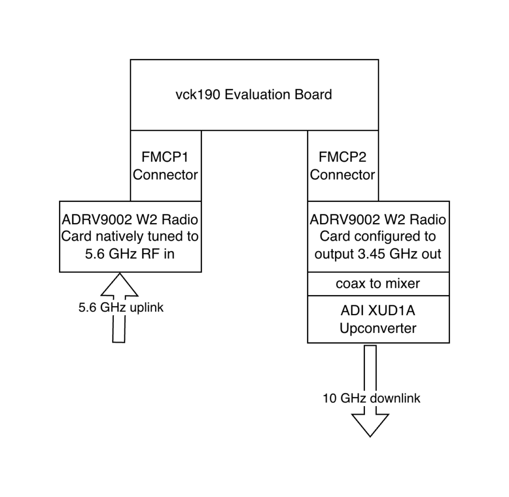
We’ve addressed the FPGA, but what about radio access? Using two identical ADRV9002 cards would simplify the software driver ecosystem. We know how to deal with the 9002. For uplink at 5 GHz, the ADRV9002 can be used directly. However, it cannot handle 10 GHz by itself. For that, we would need something like the ADI XUD1A upconverter.
See the figure for what the lab setup would look like with this configuration.
We’d use a 7.000 GHz local oscillator at 3.45 GHz IF for the transmit side. The XUD1A gives us 4 independent TX/RX channels. Since Haifuraiya has 64-channel FDMA stream multiplexed into a single TDM carrier, we only need one physical RF stream for the current downlink. This means we will have 3 spare hardware channels on the XUD1A available for multi-antenna array experiments, telemetry, useful beacons, or whatever we can come up with.
Now, there is some coax connector stuff going on here that we should not ignore. The XUD1A has different connectors than the radio cards. Adapters or additional cables may be necessary.
If you want to be a part of the team, and learn by doing through modern and innovative open source work, please visit https://openresearch.institute/getting-started and sign up.
VCK190 has safely arrived at Remote Labs West. We look forward to opening it up and getting it available in the lab. This dev board allows us to port designs to space hardware, and also gives ORI volunteers the opportunity to learn and design with the Versal chip set. We are very excited to offer this new resource to our volunteers.